- Laboratory
- Physico-chemical analysis
- Infrared spectrometer
- Bruker Nano Surfaces

- Products
- Catalogs
- News & Trends
- Exhibitions
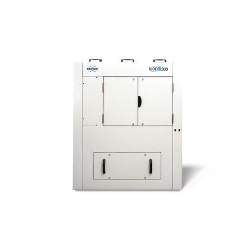
Infrared spectrometer IconIR300™ AFMinspectionfor nanotechnology
Add to favorites
Compare this product
Characteristics
- Type
- infrared, AFM
- Applications
- inspection, for nanotechnology, R&D
- Configuration
- benchtop
Description
Adds 300 mm of sample access for semiconductor R&D, failure analysis, and nanocontaminant identification
The Dimension IconIR300™ large-sample nanoIR system provides high-speed, high-accuracy nanoscale characterization for semiconductor applications, featuring unrivaled capabilities, sample size, and material type flexibility. Through its combination of proprietary photothermal IR spectroscopy and nanoscale AFM property mapping capabilities, IconIR300 enables automated wafer inspection and defect identification on the widest range of wafer and photomask samples. The system significantly extends the application of AFM-IR technology to semiconductor industry segments beyond the reach of traditional techniques.
Built on the groundbreaking large-sample architecture of the Dimension IconIR system, IconIR300 provides correlative microscopy and chemical imaging, as well as enhanced resolution and sensitivity. Integrated with automated wafer handling and advanced data collection/analysis software, the system enables greater time- and cost-savings and production efficiency.
Whole-Wafer
nanoscale chemical and material property characterization
Combines IR spectroscopy and AFM property mapping for highly accurate, non-destructive measurements of 200 mm and 300 mm wafers.
Unambiguous
identification of organic/inorganic nano-contaminants
Improves semiconductor wafer and photomask quality with photothermal AFM-IR data that directly correlates to FTIR libraries.
Automated
recipe-based measurements
Deliver user-friendly access to comprehensive data and KLARF file support.
Only the Dimension IconIR300 system provides:
Catalogs
No catalogs are available for this product.
See all of Bruker Nano Surfaces‘s catalogsOther Bruker Nano Surfaces products
Nanoscale Infrared Sprectrometers
Related Searches
- Microscopy
- Compound microscope
- Laboratory microscope
- Tabletop microscope
- Spectroscope
- Digital microscope
- Zoom microscope
- Biological microscope
- Benchtop spectroscope
- Research microscope
- Fluorescence microscope
- High-definition microscope
- Compact microscope
- Medical microscope
- Inverted microscope
- Optical spectroscope
- Research spectroscope
- 3D microscope
- Confocal microscope
- High-resolution spectrometer
*Prices are pre-tax. They exclude delivery charges and customs duties and do not include additional charges for installation or activation options. Prices are indicative only and may vary by country, with changes to the cost of raw materials and exchange rates.


