- Laboratory
- Laboratory medicine
- Inspection microscope
- Hitachi High-Technologies
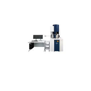
FIB-SEM microscope NX2000laboratoryfor researchinspection
Add to favorites
Compare this product
Characteristics
- Type
- FIB-SEM
- Applications
- laboratory, for research, inspection
- Ergonomics
- upright
- Observation technique
- SIM
- Resolution
2.8 nm, 3.5 nm, 4 nm, 60 nm
Description
FIB-SEM systems have become an indispensable tool for characterization and analysis of the latest technologies and high performance nano-scale materials. An ever-increasing demand for ultrathin TEM lamellas without artifacts during FIB processing require the best in ion and electron optics technologies.
Hitachi's NX2000 high performance FIB and high resolution SEM system with its unique sample orientation control* and triple beam* technologies, supports high throughput, and high quality TEM sample preparation for cutting edge applications.
* Option
Features
High contrast, real-time SEM end point detection allows ultrathin TEM sample preparation of sub 20 nm devices.
Micro sampling* and high precision positioning mechanism* enable sample orientation control for Anti-Curtaining Effects (ACE function) and uniformly-thick lamellas.
Triple Beam system* Triple beam configuration for Ga FIB-induced damage reduction.
Specifications
FIB column
Acceleration voltage - 0.5 kV - 30 kV
Beam current - 0.05 pA - 100 nA
FE-SEM column
Acceleration voltage - 0.5 kV - 30 kV
Electron source - Cold cathode field emission source
Detector
Standard detector - Upper/Lower SED & BSED
Stage - X: 0 - 205 mm
Y: 0 - 205 mm
Z: 0 - 10 mm
R: 0 - 360° infinite
T: -5 - 60°
Special accessories (Optional)
Ar/Xe ion 3rd column
Micro-sampling System
Multi-gas injection system
Double tilt system
Swing function ( for Ar/Xe ion 3rd column)
TEM sample preparation wizard
Automatic TEM sample preparation software
CAD navigation software
Linkage software with defect inspection instruments
Catalogs
No catalogs are available for this product.
See all of Hitachi High-Technologies‘s catalogsOther Hitachi High-Technologies products
Focused Ion Beam Systems (FIB/FIB-SEM)
Related Searches
- Hitachi microscope
- Compound microscope
- Hitachi laboratory microscope
- Hitachi benchtop microscope
- Control software
- Clinical chemistry analyzer
- Laboratory software
- Windows software
- Automatic clinical chemistry analyzer
- Benchtop clinical chemistry analyzer
- Digital microscope
- Acquisition software
- Data management software
- Biological microscope
- Hitachi research microscope
- Hitachi high-resolution microscope
- Compact microscope
- Random access biochemistry analyzer
- Inspection microscope
- Clinical clinical chemistry analyzer
*Prices are pre-tax. They exclude delivery charges and customs duties and do not include additional charges for installation or activation options. Prices are indicative only and may vary by country, with changes to the cost of raw materials and exchange rates.


